 |
ADS:
|
Dushu Lake Higher Education Town, Ruoshui Road 398, Suzhou Industrial Park, Suzhou |
| TEL: |
0512-62872554 |
| FAX: |
0512-62603079 |
| CODE: |
215125 |
|
 |
|
|
| |
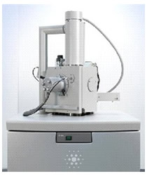
Instruments: |
Tungsten Filament SEM |
 |
Model: |
Inspect S |
Manufacturers: |
FEI, USA |
| Configuration: |
- Source: Tungsten filament
- Back-scattered electron detector |
| Specifications: |
- Voltage: 200 V to 30 kV
- Magnification: 7-1,000,000
- High-vacuum (<6e-4Pa) and low-vacuum (10-270Pa) modes
- Resolution:
High-vacuum (<6e-4Pa):
- 3.0 nm at 30 kV (SE)
- 4.0 nm at 30 kV (BSE)
- 10.0 nm at 3 kV (SE)
Low-vacuum (10-270Pa):
- 3.0 nm at 30 kV (SE)
- 12.0 nm at 30 kV (SE)
- Sample chamber: motorized x-y-z- rotate stage , 284mm |
|
| Application: |
|
Surface morphology observation in high-vacuum and low-vacuum(10-270Pa)
Contact us:
Xiong-hui Zeng: 0512-62872545; xhzeng2007@sinano.ac.cn
Lu Zhang: 0512-62872554; luzhang2007@sinano.ac.cn |
|
| |
|
